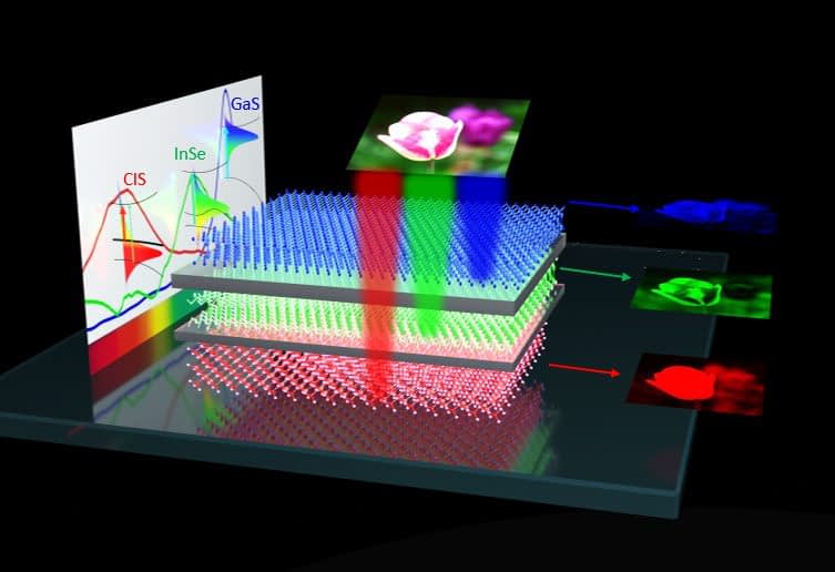
Scientists at Georgia State University have successfully developed a type of artificial vision device that could lead to the development of an “electric eye.” The new device incorporates a novel vertical stacking architecture that enables greater depth of color recognition and scalability on a micro-level.
The new research was published in the journal ACS Nano.
Eventual Microscale Cameras for Microbots
Sidong Lei is an assistant professor of physics and lead author of the research.
“This work is the first step toward our final destination-to develop a microscale camera for microrobots,” Siding Lei said. “We illustrate the fundamental principle and feasibility to construct this new type of image sensor with emphasis on miniaturization.”
The work completed by Lei’s team could lead to a biomimetic artificial vision device that uses synthetic methods to mimic biochemical processes. It could achieve this by using nanotechnology.
“It is well-known that more than 80 percent of the information is captured by vision in research, industry, medication, and our daily life,” he continues. “The ultimate purpose of our research is to develop a micro-scale camera for microrobots that can enter narrow spaces that are intangible by current means, and open up new horizons in medical diagnosis, environmental study, manufacturing, archaeology, and more.”
Biometric “Electric Eye”
This new biometric “electric eye” advances color recognition, which is the most critical vision function. This is extremely important given how conventional color sensors usually take up a large amount of physical space while offering less accurate color detection.
Ningxin Li is a graduate student in Dr. Lei’s Functional Materials Studio.
“The new functionality achieved in our image sensor architecture all depends on the rapid progress of van der Waals semiconductors during recent years,” Li says. “Compared with conventional semiconductors, such as silicon, we can precisely control the van der Waals material band structure, thickness, and other crucial parameters to sense the red, green, and blue colors.”
The van der Waals semiconductors, which rely on vertical color sensors, belong to a new class of materials in which individual atomic layers are bonded by weak van der Waals forces. They are crucial for discovering new physics and designing next-gen devices.
“The ultra-thinness, mechanical, and chemical stability of these new semiconductor materials allow us to stack them in arbitrary orders. So, we are actually introducing a three-dimensional integration strategy in contrast to the current planar micro-electronics layout. The higher integration density is the main reason why our device architecture can accelerate the downscaling of cameras,” Li says.
Patent Pending Technology
This new technology is patent pending with Georgia State’s Office of Technology Transfer & Commercialization (OTTC).
Cliff Michaels is the director of OTTC.
“As nanotechnology advances and devices become more compact, these smaller, highly sensitive color sensors will be incredibly useful,” Michaels said.
According to the researchers, the new discovery could help advance devices for the vision-impaired.
“This technology is crucial for the development of biomimetic electronic eyes and also other neuromorphic prosthetic devices,” says Li. “High-quality color sensing and image recognition function may bring new possibilities of colorful item perception for the visually impared in the future.”
“This is a great step forward, but we are still facing scientific and technical challenges ahead, for example, wafer-scale integration. Commercial image sensors can integrate millions of pixels to deliver high-definition images, but this has not been implemented in our prototype yet,” he continues. “This large-scale van der Waals semiconductor device integration is currently a critical challenge to be surmounted by the entire research society. Along with our nationwide collaborators that is where our team is devoting our efforts.”
Credit: Source link


